(China (Mainland))

Product Summary
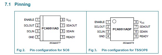
The PCA9511AD is a hot swappable I2C-bus and SMBus buffer that allows I/O card insertion into a live backplane without corrupting the data and clock buses. Control circuitry prevents the backplane from being connected to the card until a stop command or bus idle occurs on the backplane without bus contention on the card. When the connection is made, the PCA9511AD provides bidirectional buffering, keeping the backplane and card capacitances isolated. The PCA9511AD rise time accelerator circuitry allows the use of weaker DC pull-up currents while still meeting rise time requirements. The PCA9511AD incorporates a digital ENABLE input pin, which enables the device when asserted HIGH and forces the device into a low current mode when asserted LOW, and an open-drain READY output pin, which indicates that the backplane and card sides are connected together (HIGH) or not (LOW). During insertion, the PCA9511AD SDA and SCL lines are precharged to 1 V to minimize the current required to charge the parasitic capacitance of the chip.
Parametrics
PCA9511AD absolute maximum ratings: (1)ten enable tiμe [2]: 110μs; (2)tidle(READY)bus idle tiμe to READY active [1]: 50, 105, 200 μs; (3)tdis(EN-RDY)disable tiμe (ENABLE to READY): 30ns; (4)tstp(READY)SDAIN to READY delay after STOP [3]: 1.2μs; (5)tREADY SCLOUT/SDAOUT to READY delay [3]: 0.8μs; (6)ILZ(READY)off-state leakage current on pin READY VENABLE = VCC: ±0.3μA; (7)Ci(ENABLE)input capacitance on pin ENABLE VI = VCC or GND [4]: 1.9, 4.0 pF.
Features
PCA9511AD features: (1)Bidirectional buffer for SDA and SCL lines increases fan out and prevents SDA and SCL corruption during live board insertion and removal from multipoint backplane systems; (2)Compatible with I2C-bus Standard-mode, I2C-bus Fast-mode, and SMBus standards; (3)Built-in DV/Dt rise time accelerators on all SDA and SCL lines (0.6 V threshold)requires the bus pull-up voltage and supply voltage (VCC)to be the same; (4)Active HIGH ENABLE input; (5)Active HIGH READY open-drain output; (6)High-impedance SDA and SCL pins for VCC = 0 V; (7)1 V precharge on all SDA and SCL lines; (8)Supporting clock stretching and multiple master arbitration/synchronization; (9)Operating power supply voltage range: 2.7 V to 5.5 V; (10)0 Hz to 400 kHz clock frequency; (11)ESD protection exceeds 2000 V HBM per JESD22-A114, 200 V MM per JESD22-A115, and 1000 V CDM per JESD22-C101; (12)Latch-up testing is done to JEDEC Standard JESD78 which exceeds 100 mA n Packages offered: SO8, TSSOP8 (MSOP8).
Diagrams
| Image | Part No | Mfg | Description |  |
Pricing (USD) |
Quantity | ||||||||||||
|---|---|---|---|---|---|---|---|---|---|---|---|---|---|---|---|---|---|---|
 |
 PCA9511AD,112 |
NXP Semiconductors |
Buffers & Line Drivers HOTSWAP I2C/SMBUS BUFFER |
Data Sheet |
|
|
||||||||||||
|
PCA9511AD,118 |
NXP Semiconductors |
Buffers & Line Drivers HOT SWAP I2C/SMBUS |
Data Sheet |
|
|
||||||||||||
|
PCA9511ADP,118 |
NXP Semiconductors |
Buffers & Line Drivers HOTSWAP I2C/SMBUS BUFFER |
Data Sheet |
|
|
||||||||||||